SWHL-logo


Experimental verification of sub-wavelength holographic lithography (SWHL) concept

M. Borisov et. al. | Proc. SPIE Vol. 11324, Novel Patterning Technologies for Semiconductors 2020, March 2020 | Article pdf
  • Traditional photolithography relies on geometrical optics, with complex and costly technologies (like OPC and PSM) used to correct distortions in the image.
  • Sub-Wavelength Holographic Lithography (SWHL): A new, unconventional approach to lithography that reduces costs by using diffraction and interference effects to create high-quality images with fewer exposure steps.
  • SWHL Advantages: This method enables printing on 3D surfaces and significantly reduces costs while improving resolution capabilities.
  • Two systems were developed to demonstrate SWHL’s ability to print with sub-wavelength resolution and on 3D surfaces, confirming the effectiveness of the technology.


Analysis of an effect of perturbations in SWHM and illuminating optical scheme parameters on an aerial image

M. Borisov et. al. | Proc. SEMI Advanced Semiconductor Manufacturing Conference 2012, May 2012 | Article pdf
  • Introduces sub-wavelength holographic lithography (SWHL) as a novel technique for creating integrated circuit (IC) layer aerial images using defect-tolerant holographic patterns and simple optical setups.
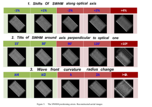
  • Simulations show the method is highly resilient to typical disturbances during mask manufacturing or photoresist exposure, ensuring reliable image quality.
  • Phase noise, caused by substrate flatness deviations, is the primary concern. However, this can be minimized by incorporating surface measurements into mask calculations.
  • Large-scale fluctuations in mask positioning and grayness function do not significantly affect image quality, thanks to the method’s inherent tolerance.
  • The precision of current manufacturing systems surpasses the critical disturbance levels, making the approach practical and effective for use.


Phase-shift at sub-wavelength holographic lithography (SWHL)

M. Borisov et. al. | Proc. Vol. 8352, 28th European Mask and Lithography Conference, April 2012 | Article pdf
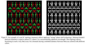
  • Advancing Sub-Wavelength Holographic Lithography (SWHL): Researchers have been refining SWHL methods for creating IC layer topologies, leveraging innovative sub-wavelength holographic masks (SWHM).
  • Advantages Over Traditional Masks:
    • Defect Tolerance: SWHMs are highly resilient to local defects, reducing the need for strict manufacturing conditions and intensive post-production verification.
    • Simplified Manufacturing: Achieving sub-wavelength resolution only requires adjusting transparency area properties (size, position, and number). Unlike traditional methods, no specialized coatings or complex phase-shifting elements are needed.
    • Versatility in Application: The SWHL approach can be used to create both test structures and real IC layer designs, showcasing its flexibility and practicality.


Experimental verification of sub-wavelength holographic lithography (SWHL) concept

M. Borisov et. al. | Proc. SPIE Vol. 11324, Novel Patterning Technologies for Semiconductors, MEMS/NEMS and MOEMS 2020, March 2020 | Article pdf
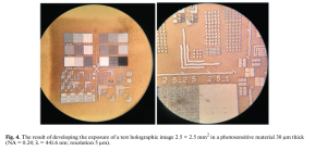
 

  • Simplified Optical Setup: Unlike conventional systems, SWHL eliminates the need for complex projection optics, using a simple illuminator with just a few optical elements.
  • Experimental Success:
  • Sub-Wavelength Resolution: Achieved a critical dimension (CD) of 250 nm using a 442 nm wavelength laser, demonstrating resolutions below the wavelength (0.56λ).
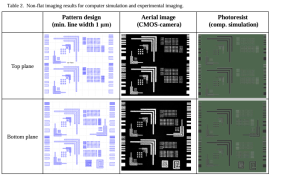
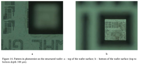
  • 3D Imaging Capability: Developed a tool that generated multi-plane images with a depth of 100 μm and resolution of 2 μm using NA 0.24.
  • Reliable Simulation and Validation: Experimental results closely matched computer simulations, confirming the accuracy of the software and the robustness of the SWHL method.


Effective Methods of Synthesis and Optimization of a Holographic Mask

V. Chernik et. al. | Doklady Physics, Vol. 68, p328-333, February 2024 | Article pdf

  • The synthesis of holographic masks is framed as an optimisation problem to improve holographic image quality. A fast and efficient algorithm based on FFT is used for mask synthesis.
  • A scalable software tool has been developed to design holographic masks for various applications, including MEMS, MOEMS, and advanced chip production.
  • The software can synthesize holograms for complex 3D images and optimize the depth of focus in optical systems.
  • Experimental Validation:
  • Holographic masks designed with the software were manufactured using an electronic lithograph and tested in optical setups.
  • Successful imaging in thick photoresists (10–50 μm) was achieved at a reconstruction wavelength of 441.6 nm, demonstrating the system’s capability.


Mathematical problems of holographic mask synthesis

M. Borisov et. al. | Proc. SPIE Vol. 11324, Novel Patterning Technologies for Semiconductors, MEMS/NEMS and MOEMS 2020, March 2020 | Article pdf
  • Holographic Lithography Advancements: Nanotech SWHL developed innovative algorithms to synthesize holographic masks for applications like MEMS, MOEMS, and high-end IC production.
  • Efficient Algorithms: Leveraged FFT-based synthesis algorithms with complexity O (N ln⁡N) to generate masks for any IC layer, enabling efficient and scalable mask creation.
  • Enhanced Image Quality: Introduced a continuous phase-shifting optimization method using WFS, DFS, and gradient descent. By altering amplitude and phase distributions, the synthesized masks produce higher-quality images of the original pattern, similar to other Resolution Enhancement Techniques (RET).
  • Sustainability and Accessibility: Modern computing clusters allow the efficient synthesis of holographic masks, which can now be implemented in cost-effective, sustainable devices for photolithography.
  • Practical Applications: Addressed and solved challenges of traditional projection photolithography, such as 3D imaging and image quality optimization, through a fully numerical approach.


Maskless holographic schemes based on phase micromirror SLMs

M. Borisov et. al. | Proc. SPIE Vol. 11324, Novel Patterning Technologies for Semiconductors, MEMS/NEMS and MOEMS 2020, March 2020 | Article pdf

  • Utilizes phase micromirror Spatial Light Modulators (SLMs) to eliminate traditional projection masks and lenses, simplifying lithography for MEMS, MOEMS, and advanced semiconductors.
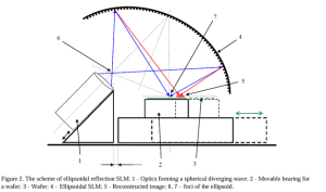
  • Achieves up to 0.9 numerical aperture (NA) using non-planar reflective SLMs, enabling advanced imaging capabilities without immersion.
  • Novel methods convert amplitude to phase holograms, supporting precise and cost-effective maskless lithography.
  • Scalable and Versatile: Suitable for industrial wafer sizes, but further research on pixel gap effects and modelling is needed to enhance image quality.