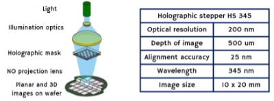
HoLiSTEP aims to demonstrate the potential of sub-wavelength holographic lithography as a disruptive technology for high-resolution 2D and 3D semiconductor and micro component devices manufacturing. Holographic lithography has the potential to overcome limitations of projection lithography and enables:
- Unique capability to produce high-resolution 3D structures in one single exposure
- Significant cost reduction for photomasks and equipment production
- Infinite lifetime of holographic photo-masks
- Applicability across all technology nodes
- The realisation of maskless lithography

Key to the sub-wavelength holographic lithography process are holographic masks which have several substantial advantages in comparison with the traditional projection lithography masks. In holographic lithography, each point of an image is composed as a superposition of wavefronts coming from all elements on the mask. This means that a much larger number of local defects on the mask can be tolerated before the image quality is impacted. Consequently, the lifetime of holographic masks is significantly increased and the required maintenance work decreased compared to projection lithography. This also reduces the waste produced during manufacturing processes.
Since the holographic masks simultaneously operate as projection optics, there is no need for complex projection lenses in holographic tools, making them much simpler and less expensive to produce compared to projection lithography tools.

All these features of the new technology enable versatile manufacturing of 3D structures. In the future, we plan to add another product to the line of holographic steppers, which operates at 288nm wavelength. This tool would have sufficient resolution to produce integrated circuits. The lower cost for and higher versatility of the holographic stepper will encourage the emergence of new players in the market of IC production and empower the production of principally new IC topologies currently not possible with projection lithography.
During the project, the HoLiSTEP consortium will build and demonstrate an industrial prototype for the holographic stepper operating at a wavelength of 345nm (HS-345) with 200nm resolution.
We will demonstrate high-resolution 2D and 3D semiconductor and micro component manufacturing with optimized costs and broad production capabilities.
Several technical advancements need to be made to realise this ambitious goal.
- A custom-tailored alignment system will provide the necessary precision when aligning wafers to the holographic mask. To produce a desired micro structure, mask and wafer need to be precisely aligned with each other before exposing to the laser. A misalignment would yield an unusable structure. Due to the difference between projection masks and holographic masks, alignment systems used in projection lithography are not suitable in holographic lithography as the image is created by interference of light rather than acting as a stencil.
- An adaptive optics system. As the optical systems in holographic lithography are greatly simplified by the holographic masks and much simpler illumination optics suffice, aberrations of the wavefronts can happen and thus need to be corrected.
- A high-energy/high power UV fiber-based laser with large temporal/spatial coherence. Due to the differences to projection lithography, lasers commonly used are not applicable to holographic lithography. While projection lithography focuses on illumination uniformity, pupil shaping, spatial coherency control, holographic lithography requires specific phase and intensity distribution of the coherent light wave on the holographic mask. Such a laser is not commercially available at the moment and will be developed in the project.
These subcomponents will then all feed into the design and production of the first industrial prototype of a holographic lithography stepper. To operate this tool, a control system integrating all separate components will be designed. Additionally, new software modules for vector diffraction models with controllable rigidity and photoresist exposure models need to be developed and integrated in the current software package to enable production of various structures.
Using the completed industrial prototype, several studies will be conducted:
- Demonstration of holographic lithography capabilities by producing selected structures. Using our insights into real-world requirements, we will compile a set of 2D and 3D structures that will be produced with the holographic stepper. Such a production includes the refinement of production processes and materials to be compatible with holographic lithography. The selected structures will include features that cannot be produced in projection lithography, for example sloped walls, curved surfaces and multi-level structures.
- Provide evidence that holographic masks have a high defect tolerance. During the production of selected structures, special attention will be paid to the quality of the produced structures and any potential deterioration with repeated mask usage. While computer simulations have identified that up to 1% of the mask area can have defects before the image quality will be negatively impacted, HoLiSTEP will deliver the first practical demonstration of this feature.
- Assess the high-throughput potential of the HL technology in an operational environment. In industry use, lithography needs to be a high-throughput process to satisfy the customer needs. While a full demonstration of high-throughput capabilities requires additional equipment such as a robotic arm for quick wafer changes, assessment of the production time for one wafer will allow a calculation of how many structures could potentially be produced per hour. This information will be key when doing a comparison to current production methods and highlighting the capabilities of the technology to end users.
Aside from the technical work, the project will also evaluate the impact of the novel disruptive technology on the environment. This will also give insights into aspects that need attention towards a sustainable and green manufacturing process.
While a lot of the benefits of holographic lithography lie in the extended production capabilities, there also is an environmental impact to be considered. Projection lithography produces enormous amounts of waste and uses some toxic chemicals. Especially the extreme sensitivity of projection masks to defects means they need to be changed after around 130 hours of usage, while holographic masks have a virtually unlimited lifetime. Simpler optical systems also mean fewer lenses: instead of around 15 lenses in projection lithography, only 1-2 lenses are used in holographic lithography. During our project, we aim to thoroughly quantify the environmental impacts or holographic lithography through an integrated life cycle assessment.

