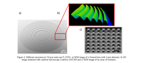
2.5D-Patterning via i-line grayscale exposure for photonic structures and micro lens arrays
S. Schermer et. al. | Proc. SPIE 12956, Novel Patterning Technologies 2024, April 2024 | Article pdf
- Grayscale Patterning Approach: The paper presents a patterning method using i-line grayscale exposure with a NIKON NSR2205i11D stepper and specialized grayscale reticles.
- Photoresist and Process: The positive tone ma-P 1275G photoresist from Micro Resist Technology, covering 5 μm to 14 μm thickness, is utilized for lithographical pattering on 150mm wafers to create various 2.5D structures.
- Characterization and Process Setup: Generated 2.5D grayscale patterns are characterized using stylus profilometry, AFM, SEM, and confocal microscopy. The paper discusses setting up the grayscale exposure process and the iterative adaptation of the grayscale reticle.
- Potential use of Holographic Lithography for fabrication of 2.5D and nanostructures and the integration of the Holographic Lithography process in a complex fabrication chain especially for Grayscale Lithography.
Characterization of negative tone photoresist mr-EBL 6000.5 for i-line stepper and electron beam lithography for the Intra-Level Mix & Match Approach
S. Schermer et. al. | Micro and Nano Engineering, Vol. 23, June 2024, 100264 | Article pdf
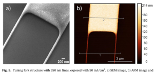
- Photoresist evaluation of mr-EBL 6000.5: The paper focuses on the evaluation of mr-EBL 6000.5, a chemically amplified negative tone resist suitable for an Intra-Level Mix & Match (ILM&M) lithography approach.
- ILM&M Approach: This technique integrates multiple exposure technologies on the same resist layer, allowing for the resolution of diverse pattern dimensions while minimizing process steps and time.
- Process Optimization: Investigation of process parameters for both i-line stepper lithography and electron beam lithography (EBL) is conducted, including a spin curve, post-exposure bake (PEB) studies, and analysis of minimum feature sizes, leading to optimized conditions for the ILM&M approach.
- Potential use of Holographic Lithography for photoresist evaluation and process integration of fabrication for nanostructures and the integration of the Holographic Lithography process in a complex fabrication chain.
Intra-level mix and match lithography with electron beam lithography and i-line stepper combined with resolution enhancement for structures below the CD-limit
C. Helke et. al. | Micro and Nano Engineering, Vol. 19, June 2023, 100189 | Article pdf
- Intra-level Mix & Match (ILM&M) Approach: The paper explores combining electron beam lithography (EBL) and i-line stepper lithography on the same resist layer, leveraging the strengths of both methods.
- Negative Tone Resist ma-N 1402: The study uses ma-N 1402, a UV and electron-sensitive negative tone resist, for both EBL and ILM&M processes, allowing for effective patterning.
- Patterning and Results: Inspection via scanning electron microscopy (SEM) confirmed a 1:1 print for both lithography techniques, achieving structures down to 86 nm width by varying the i-line stepper exposure dose.
- Potential use of Holographic Lithography for photoresist evaluation and process integration of fabrication for nanostructures and the integration of the Holographic Lithography process in a complex fabrication chain.
Integration of (Poly-Si/Air)n Distributed Bragg Reflectors in a 150mm Bulk Micromachined Wafer-Level MOEMS Fabrication Process
C. Helke et. al. | Micro and Nano Engineering, Vol. 19, June 2023, 100189 | Article pdf
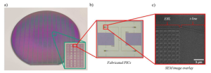
- Development of (Poly-Si/Air)n Distributed Bragg Reflectors (DBR) into a MOEMS Fabry-Pérot Interferometer (FPI) concept at 150mm wafer scale, offering a resource-efficient alternative to traditional Ion-Assisted Deposition DBRs.
- Integration in MOEMS FPIs: The (Poly-Si/Air)n DBRs can be integrated into two movable reflector carriers made from individually fabricated bonded wafers, enhancing the functionality of MOEMS FPIs.
- Reflectance Performance: Investigated as (HL) and (HL)² reflector stacks, the (Poly-Si/Air)n DBRs demonstrate a reflectance exceeding 91% in the wavelength range of 2.8–5.7 μm, highlighting their effectiveness in optical applications.
- Potential use of Holographic Lithography for fabrication of nanostructures and the integration of the Holographic Lithography process in a complex fabrication chain.
Combining nano-scale imprint lithography and reactive ion etching to fabricate high-quality surface relief gratings
M. Haase et. al. | Proceedings Vol. 12898, Advanced Fabrication Technologies for Micro/Nano Optics and Photonics XVII, March 2024 | Article pdf
- VR and AR related photonic structure fabrication of TiO2 Surface Relief Gratings (SRG) with 200nm Lines and Spaces via Nanoimprint Lithography (NIL) and Reactive Ion Etching (RIE) at 150mm wafer scale and glass substrates
- Fabrication process development and integration for high volume manufacturing of these Nanostructures
- Potential use of Holographic Lithography for fabrication of nanostructures and the integration of the Holographic Lithography process in a complex fabrication chain
Tunable Fabry-Pérot interferometer integrated in a silicon waveguide of an on-chip optical platform for long infrared wavelengths
J. Wecker et. al. | Proc. SPIE Vol. 12426, March 2023 | Article pdf
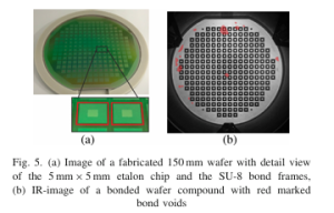
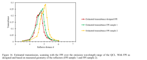
- Realization of a Tunable Fabry-Pérot Interferometer (FPI) integrated on-chip for long infrared (IR) wavelengths, featuring two parallel Bragg reflectors at the ends of silicon waveguides suspended in air.
- Performance Evaluation of a (Si/Air)² layer stack achieves a 270 nm full width half maximum and over 25% peak transmittance at 9.4 μm, evaluated through simulations and measurements.
- Fabrication process development of the integrated in-plane FPI and a MEMS actuator at 150mm wafer scale.
- Potential use of Holographic Lithography for fabrication of nanostructures and the integration of the Holographic Lithography process in a complex fabrication chain.
On the Fabrication and Characterization of Polymer-Based Waveguide Probes for Use in Future Optical Cochlear Implants
C. Helke et. al. | Materials 2023, 16, 106 | Article pdf
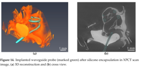
- Fabrication of optical Cochlear Implants (oCIs): The paper discusses advancements in hearing restoration through oCIs that excite optogenetically modified spiral ganglion neurons (SGNs) with optical pulses guided via flexible polymer-based waveguide probes.
- Waveguide Probe Fabrication: Utilizes 150mm wafer-level micromachining processes, including lithography for spin-coating cladding and waveguide layers (SU8 and PMMA), along with etching and integration of adhesion and metal layers for laser diode bonding.
- Performance Testing and Proof-of-Concept: Optical microscopy and SEM confirm smooth waveguides for low-intensity light loss. The probes were tested in single-beam guides (SBGs) in animal models, demonstrating the feasibility of optical stimulation in cochlear implants.
- Potential use of Holographic Lithography for fabrication 2.5D structures and the integration of the Holographic Lithography process in a complex fabrication chain.
Multichannel laser diode to polymer waveguide array coupling with a double-aspheric lens
K. Kunze et. al. | Applied Optics Vol. 62, Issue 35, pp. 9353-9360 (2023) | Article pdf
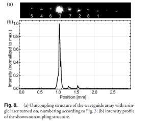
- Multichannel Optical System Development: The paper presents an optical system for coupling laser arrays to polymer waveguide array probes using a single biconvex lens, enabling efficient multichannel operation.
- Cylindrical Module Design: A cylindrical module with 13 mm diameter and 20 mm length couples eight optical channels with crosstalk below -13 dB, achieving quasi-uniform coupling for a waveguide array with a 100 µm lateral facet pitch.
- Waveguide Technology and Prototype Evaluation: The polymer waveguide technology allows for tapering the lateral pitch to 25 µm at the tip, utilizing SU8 and PMMA as core and cladding materials, designed for preclinical evaluation of optical neural stimulators.
- Potential use of Holographic Lithography for fabrication 2.5D structures and the integration of the Holographic Lithography process in a complex fabrication chain.
CNT-PUFs: Highly Robust and Heat-Tolerant Carbon-Nanotube-Based Physical Unclonable Functions
S. Böttger et. al. | Nanomaterials 2023, 13(22), 2930 | Article pdf
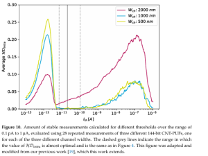
- Robust CNT-Based Physical Unclonable Function (PUF): The study investigates a unique PUF utilizing the stochastic assembly of single-walled Carbon Nanotubes (CNTs) within 200mm wafer-level technology, showcasing high robustness.
- Exceptional Performance Characteristics: The CNT-based PUFs exhibit an average fractional intra-device Hamming distance below 0.01 across a temperature range of 23 °C to 120 °C, attributed to low activation energies of less than 40 meV.
- Error Correction Efficiency: With minimal unstable bits, the devices facilitate lightweight error correction by selecting stable cells, reducing the need for complex error correction methods, demonstrating their potential as effective hardware security primitives.
- Potential use of Holographic Lithography for fabrication of nanostructures and the integration of the Holographic Lithography process in a complex fabrication chain.